2. Background
A. Basic of Memory Devices and Systems
Increased memory bandwidth and capacity requirement.
Typically, Mem chip are integrated and installed as Dual In-line Memory Module(DIMM)
DIMM’s energy consumption is significant.(20% ~ 40% of entire system power consumption)
PCM Pros,
Ability to scale down,
Low power consumption(1/3 of DRAM in operating state, zero idle state),
Non-volatility,
Fast read perf
PCM Cons,
Low write performance(SET, RESET 150ns)
Liminited cell endurance(10^6 – 10^8)
The focus in this paper is the duet of performance and energy consumption, so endurance problem is outside the scope of this work
3. DRAM/PCM Hybrid main memory architecture

A. Using DRAM as a Write Buffer Memory
DRAM Buffer is large enough to absorb all incoming write data from LLC without ever being completely full, then overall perfomance same as DRAM system
First Challenge, the number of entries in the buffer that can absorb all incoming traffic should be accurately estimated.
DRAM buffer need not be infinitely size. (Upper bound in most case)
High hit ratio in L1/L2 caches So, only few of the memory request through to DRAM buffer
But, complex indexing and data-searching algorithm to handle the next incoming request. If requested data is stored whthin the DRAM buffer and has not yet been flushed to the PCM, then request must be served from the DRAM buffer to coherency
Second Challenge, DRAM buffer system consume less energy than large size DRAM system. But, temporarily hold data until the slower PCM can eventually absorb this data
One data-write request, initial DRAM write and potentially one DRAM read followed by one PCM Write. So, duplicated Write operation and additional read operation will increase energy.
The DRAM buffer hit ratio is not so high(0.6% ~ 2%)
B. Using DRAM as a Cache
Request served directly from the DRAM cache(i.e. DRAM hits), the PCM is only accessed on a DRAM cache miss.
If the hit ratio of DRAM cache is high enough to reduce the number of PCM accesses, the additional DRAM read and PCM write operation due to cache flush can be reduced. Consequenctly, the energy consumption will decrease, as compared to DRAM buffer architecture
Since PCM’s read performance is similar to DRAM. But, perforamcne penalty incurred when there is a cache miss that result in a PCM write operation is quite serve and cannot be avoided. This case is Flusing of dirty block(“dirty miss”)
Overall cache miss penalty is primarily determined by the number of dirty miss.
Performance degradation = (Tmiss = Nwb x Tblock), Nwb and Tblock indicate the total number of dirty misses that lead to a PCM write, and the time to write one DRAM cache line to the PCM

Hit ratio of DRAM cache is higher than that of DRAM bufffer(Fig 2.)
Increasing the cache size enhances the cache hit ratio without any side effect, But, increasing the cache block size has an adverse effect on the miss penalty.
Therefore, in regular cache configurations, the optimal block size (in terms of total miss penalty) is 64 bytes, even though its corresponding cache hit ratio is not the highest possible
We can employ a DRAM cache that will be used only for wirte operations.(decrease hit ratio and miss penalty)
The read misses in the DRAM cache do not force a cache block replacement. Instead, the missed block is served directly from the PCM without allocating a block in the DRAM cache.
The performance of this configuration is still not as high as when using a DRAM buffer architecture, due to the heavy miss penalty of dirty write-back operations
But, a high miss rate in the DRAM cache has caused the memory write queue to fill up.
C. A DRAM Cache Architecture Supporting Threshold-based Pre-Invalidation
In Fig 3,
DRAM buffer = better performance(large size), worse energy consumption(duplicate write)
DRAM cache = worse performance(dirty miss), better energy consumption
Our proposed scheme utilizes the DRAM as a cache in order to reduce the number of memory accesses to the PCM, but with modifications targeting a reduction in the miss penalty due to dirty misses.
The incoming data must wait until a possibly lengthy flush-out process is completed. So, In order to hide this flush-out time substantially, our proposed cache is designed to always have a room for incoming data.
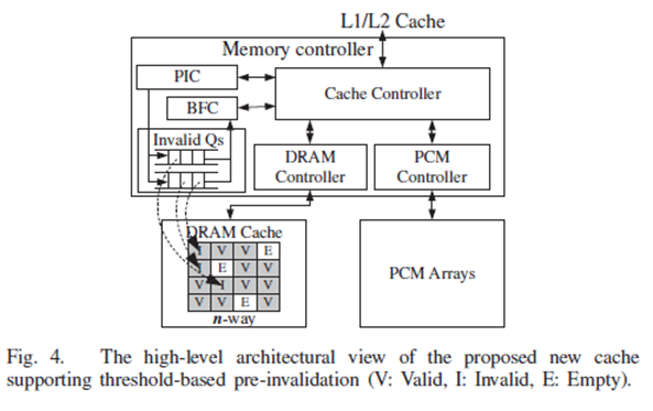
Threshold-Based Pre-Invalidation(TBPI)
Write-only DRAM cache
Two level of flush-out queues
Threshold-based pre-invalidation
This methodology minimizes the stall time due to DRAM cache misses by increasing the memory bus utilization while considering the PCM’s poor write performance.
Each set always has at least one empty block
The Pre-Invalidation Controller (PIC), which is embedded within the memory controller, invalidates at least one data block from a particular set in the DRAM cache, before the set is full.
If the PCM module is busy when a DRAM cache block is invalidated, the PIC adds the physical address of the invalidated block into Queue 0 or 1, depending on the remaining number of empty blocks. If there is no available block in a set, the address is placed into Queue 0, the urgent queue, which has the highest flush-out priority. Otherwise, the address is placed into Queue 1, whose priority is lower than that of Queue 0.
Background Flush Controller (BFC) evicts the data listed in the queue from the DRAM cache into the PCM. This process occurs at periods when the PCM and DRAM are not used for regular data service.
The requirement of maintaining at least one empty block per set may not always be satisfied. However, we found that this scenario is extreme and happens rarely, even if we set the threshold value to just one.
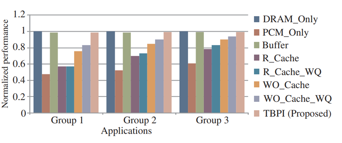
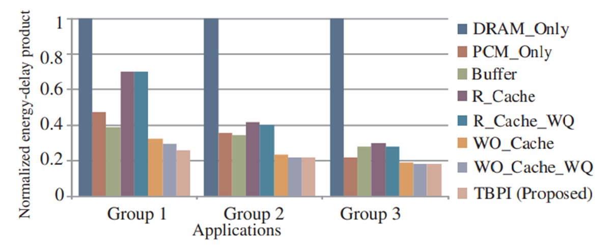
4. Experimental Evaluation

5.Conclusion