Latency Components : Basic DRAM Operation
CPU -> Controller Transfer time
Controller latency
Queuing, scheduling delay
Access converted to basic commands
Controller -> DRAM Trasfer time
DRAM bank latency
Simple CAS(cloumn address strobe) if row is "open" OR
RAS (row address strobe) + CAS if array precharged OR
PRE + RAS + CAS (wortst case)
DRAM - > Controller Transfer time
Bus lantency(BL)
Controller to CPU Transfer time
Multiple Bank(Interleaving) and Channels
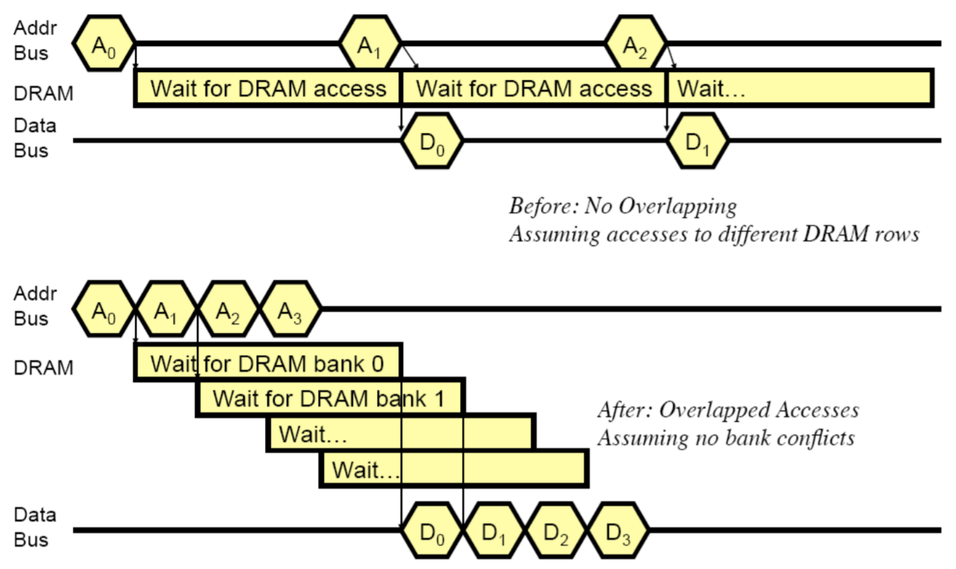
Multiple Banks
Concurrent DRAM Access를 가능하도록 함
주소내의 Bits가 주소의 위치가 어떤 Bank에 있는지 나타낸다.
Multiple independent channels serve the same purpose
그러나 별도의 Data Bus가 존재한다.
Bus의 대역폭이 증가한다.
더 높은 Concurrency를 가지려면 Bank Conflicts, Channel Conflict를 피해야 한다.
Address에서 Bank/Channel Index를 Select/Randomize 하는 방법
Low order bits는 더 많은 Entropy를 가진다.
Randomizing hash functions(i.e XOR of diff address bits)
Address Mapping (Single Channel)
Single-Chaneel 시스템은 8 byte memory bus를 가진다. (64bit)
2GB, 8 Banks, 16K row, 2K columns per bank
Row interleaving

연속적인 Bank에 연속적인 Row
파이프라인 방식으로 서비스되는 연속된 캐시블록에 대한 Access가 가능하다.
Cache block interleaving

연속적인 bank에 연속적인 Cache block, 64byte의 Cache block
연속적인 Cache block에 대한 Access는 병렬적으로 서비스 가능하다.
Bank Mapping Randomization

DRAM 컨트롤러는 주소 매핑을 무작위로 지정할 수 있다.
가능성을 줄인다,
Virtual -> Physical Mapping

OS는 DRAM에서 주소가 매핑되는 위치에 영향을 준다.
OS는 Virtual Page가 매핑되는 Bank/Channel/Rank에 영향을 줄 수있다.
More on Reducing Bank Conflicts
Subarray-Level Parallelism
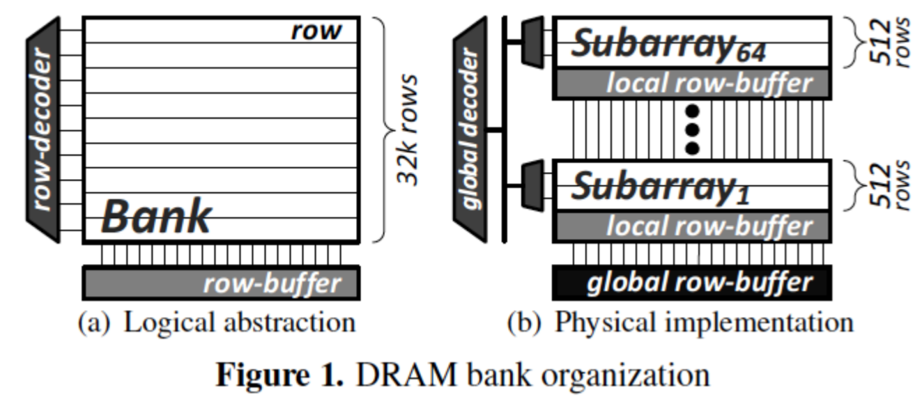
하나의 Bank는 64개의 Subarray로 구분 가능하고 Logical row-buffer가 존재한다.
(https://users.ece.cmu.edu/~omutlu/pub/salp-dram_isca12.pdf)
'개인 공부 > 메모리' 카테고리의 다른 글
| MSHRs(Miss Status Holding Register) (1) | 2021.06.10 |
|---|---|
| DRAM Operation, Memory Control & Memory Latency - 3 (2) | 2021.06.08 |
| DRAM Operation, Memory Control & Memory Latency - 1 (2) | 2021.06.07 |
| 메모리 타이밍 (0) | 2021.03.09 |
| 메모리 기초 (0) | 2021.03.09 |